
 * Encompasses everything except
* Data and Address Flops
* Control logic
* Multi-bank logic
* Arranges ports
* Port 0 is left/bottom
* Port 1 is right/top
## Port Data
* Encapsulates all of the datapath logic for a rw, w, or r port
* Sense amplifiers (read types)
* Write drivers (write types)
* Column mux (if any)
* Precharge (read or write type) (write to not destroy half selected cells in a row)
* Also includes a precharge for the replica columns
## Port Address
* Encapsulates the row decoder and wordline driver for easier placement next to a bank
* Each port will have its own port\_address module
## Plain Bitcell Array
* Encompasses everything except
* Data and Address Flops
* Control logic
* Multi-bank logic
* Arranges ports
* Port 0 is left/bottom
* Port 1 is right/top
## Port Data
* Encapsulates all of the datapath logic for a rw, w, or r port
* Sense amplifiers (read types)
* Write drivers (write types)
* Column mux (if any)
* Precharge (read or write type) (write to not destroy half selected cells in a row)
* Also includes a precharge for the replica columns
## Port Address
* Encapsulates the row decoder and wordline driver for easier placement next to a bank
* Each port will have its own port\_address module
## Plain Bitcell Array
 * 2D Array of bit cells
* Each row alternately flips vertically
* Assume bitcells tile
* Boundary is determined by boundary layer in GDS
* Word line must abut
* Bit lines must abut
## Variations of Bitcells Needed
* Normal bitcell for data storage
* Replica bitcell that is fixed to output a 0 value
* Dummy bitcell with bitlines disconnected (purely for wordline load and lithography regularity)
* 2D Array of bit cells
* Each row alternately flips vertically
* Assume bitcells tile
* Boundary is determined by boundary layer in GDS
* Word line must abut
* Bit lines must abut
## Variations of Bitcells Needed
* Normal bitcell for data storage
* Replica bitcell that is fixed to output a 0 value
* Dummy bitcell with bitlines disconnected (purely for wordline load and lithography regularity)
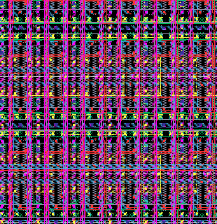
 ## Replica Bitcell Array
* Bitcells: B=regular, D=dummy, R=replica
* Main bitcell array ( $\color{green}{\textrm{green}}$ )
* Replica cols for each read port ( $\color{skyblue}{\textrm{blue}}$ ) on left or right (any number)
* Dummy bitcells on the top, bottom, left, and right for lithography regularity ( $\color{red}{\textrm{red}}$ )
* Replica columns activate two replica bitcells
* $\color{blue}{\textrm{One}}$ driven by replica wordline
* $\color{royalblue}{\textrm{Second}}$ driven by one of the normal wordlines (dark blue)
* Second port word and bit lines not shown
* Would be on right and top
## 1D Arrays
## Replica Bitcell Array
* Bitcells: B=regular, D=dummy, R=replica
* Main bitcell array ( $\color{green}{\textrm{green}}$ )
* Replica cols for each read port ( $\color{skyblue}{\textrm{blue}}$ ) on left or right (any number)
* Dummy bitcells on the top, bottom, left, and right for lithography regularity ( $\color{red}{\textrm{red}}$ )
* Replica columns activate two replica bitcells
* $\color{blue}{\textrm{One}}$ driven by replica wordline
* $\color{royalblue}{\textrm{Second}}$ driven by one of the normal wordlines (dark blue)
* Second port word and bit lines not shown
* Would be on right and top
## 1D Arrays
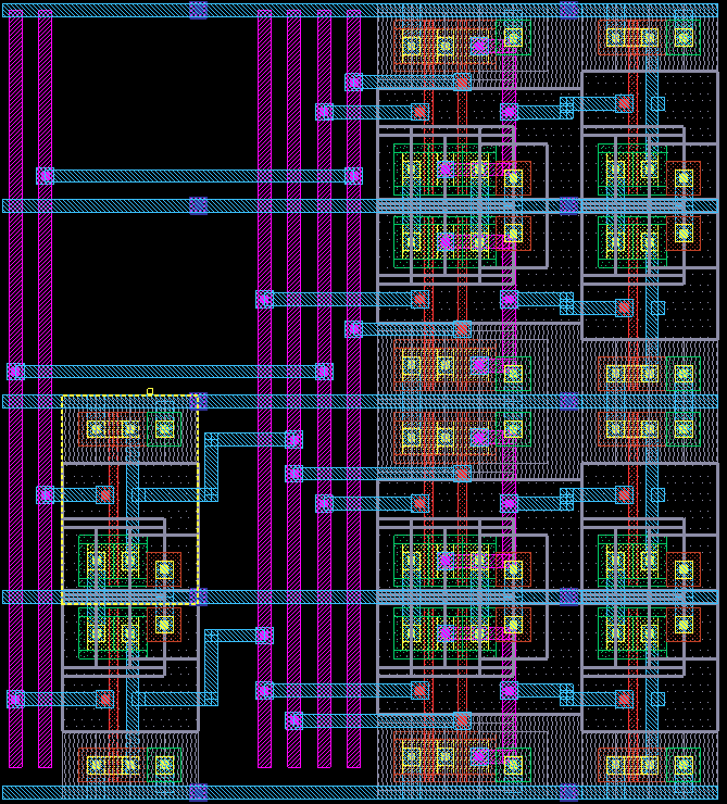
 * Several modules have 1D arrays:
* `sense_amp_array`
* `write_driver_array`
* `precharge_array`
* `single_level_column_mux_array`
* `tri_gate_array`
* `wordline_driver` (*should change name to _array)
* `sense_amp_array`, `write_driver_array`, `tri_gate_array` match column mux stride to space out
* Wish list: Allow wide sense amplifier array to use multiple rows of sense amplifiers.
* Several modules have 1D arrays:
* `sense_amp_array`
* `write_driver_array`
* `precharge_array`
* `single_level_column_mux_array`
* `tri_gate_array`
* `wordline_driver` (*should change name to _array)
* `sense_amp_array`, `write_driver_array`, `tri_gate_array` match column mux stride to space out
* Wish list: Allow wide sense amplifier array to use multiple rows of sense amplifiers.
 ## 2D Arrays
* Regular DFF arrays (`dff_array.py`)
* Buffered DFF arrays (`dff_buf_array.py`)
* Inverted DFF array (`dff_inv_array.py`)
* Can be $1*N$ or $N*1$ or $M*N$
* Wish list: $M*N$ routes pins to edges
## 2D Arrays
* Regular DFF arrays (`dff_array.py`)
* Buffered DFF arrays (`dff_buf_array.py`)
* Inverted DFF array (`dff_inv_array.py`)
* Can be $1*N$ or $N*1$ or $M*N$
* Wish list: $M*N$ routes pins to edges
 * Configurable fanout and stages
* `[4,4,4]` means 3 FO4 stages
* `[1,1,4,4]` means 2 FO1 stages followed by FO4
## Hierarchical (Address) Decoder
* Configurable fanout and stages
* `[4,4,4]` means 3 FO4 stages
* `[1,1,4,4]` means 2 FO1 stages followed by FO4
## Hierarchical (Address) Decoder
 * Generic `hierarchical_predecode` class
* Places routing rails and decode inverters
* Derived to implement multiple predecoders
* `hierarchical_predecode_2x4`
* `hierarchical_predecode_3x8`
* `hierarchical_predecode_4x16`
* Hierarchical decoder uses predecoder + another decode stage
* Predecoders are also used for the column mux decode and bank select decode
* Wish list: Handle thin bitcell height
* Generic `hierarchical_predecode` class
* Places routing rails and decode inverters
* Derived to implement multiple predecoders
* `hierarchical_predecode_2x4`
* `hierarchical_predecode_3x8`
* `hierarchical_predecode_4x16`
* Hierarchical decoder uses predecoder + another decode stage
* Predecoders are also used for the column mux decode and bank select decode
* Wish list: Handle thin bitcell height